Panta rhei. Materials science and its view of the dynamics of the world

Panta rhei. Materials science and its view of the dynamics of the world

Heraclitus’ Greek aphorism, according to which everything flows, takes on additional significance in the field of materials science. The principle of eternal becoming and change can be translated here as meaning that nothing is truly fixed and, contrary to expectations, some things are not really sharply separated. This is a unique perspective on the structure of materials and their relationships, on the interplay between substances and things. And what all this has to do with the production of modern microchips, which are found in our smartphones and smartwatches, will be discussed on the following pages.

At first, it makes sense to introduce the subject itself: Materials science is a discipline that lies between chemistry, physics, and engineering, linking these fields in a unique perspective. It is therefore an interdisciplinary field that deals with the research, development, and application of materials. As a science that focuses on materials, it aims to understand mixtures of substances, their interactions, and the resulting properties. It deals with chemical descriptions as well as physical, chemical, and mechanical characterizations, analyses of the structures and composition of substances, and the manufacturing conditions described by factors of thermodynamics and kinetics. The focus is therefore on thermodynamic and kinetic fundamentals for materials that are important in engineering:  approaches are developed through the creation of phase diagrams, the investigation of diffusion processes, and the characterization of internal interfaces.

Furthermore, one subfield of materials science deals with the development of new or adapted materials with specific properties that are tailored to the requirements of certain applications. When we think of the highly specialized materials used in modern microelectronics, for example, which form the basis for miniaturization and increased performance, it becomes clear how materials science taps into innovative potential through its combination of natural science and engineering approaches. This also demonstrates the bridge between basic research and its transfer into application-oriented reality, which is particularly important as a productive link between research and development for universities of applied sciences. 

How do materials scientists work?

Phase diagrams, i.e., representations of phase transitions as a function of various parameters, are useful for understanding the properties of substances and how they change in different states. In these diagrams, phase transitions (from solid to liquid to gas, etc.) are represented by influencing factors such as composition and temperature. The substances or individual components have different relevant properties depending on their state and, among other things, during the transitions, which need to be characterized. These diagrams can be used to investigate thermodynamic and kinetic behavior, which can then be used specifically in manufacturing processes, for example.

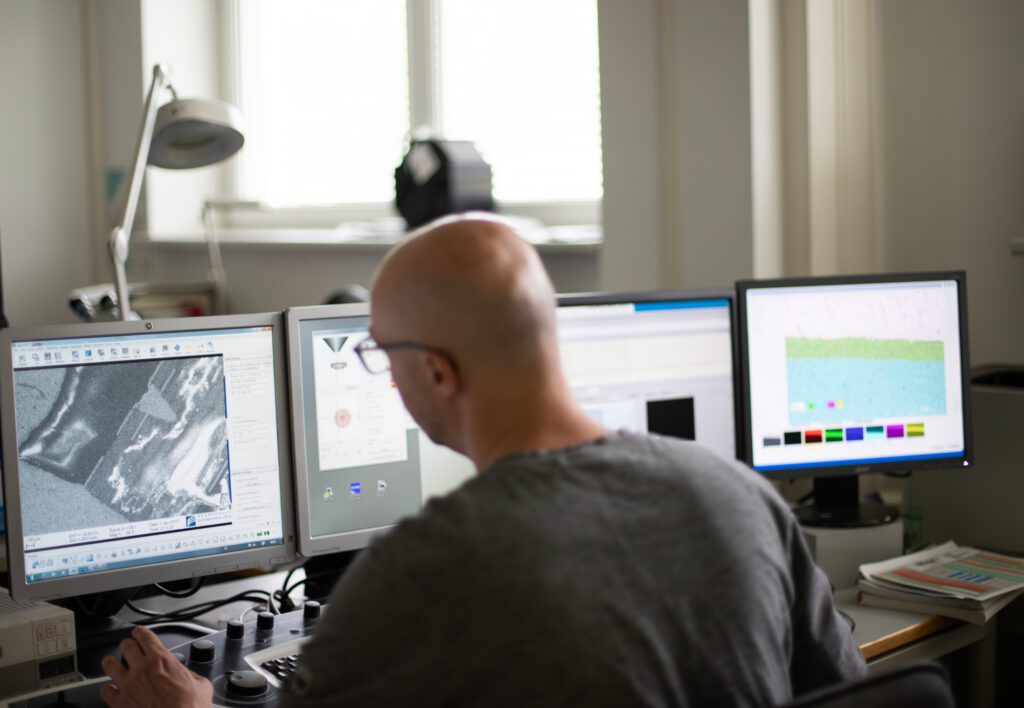
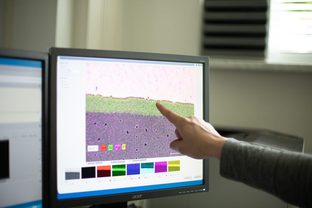
Another aspect within materials science is diffusion, i.e., the interactions between substances, for example, between two metal layers. Our everyday understanding suggests that there are no interactions between the two metals, as both are solid bodies that exist completely separately. However, if we use low-scale observation methods such as electron microscopes, in which the atoms and atomic lattices become visible, the picture changes: to stay with our example, relationships can exist between the metals, which can lead, among other things, to mutual mixing or even to the incorporation of one substance by the other. When different metals and alloys are combined, as in microchip manufacturing in electrical engineering, such effects must be taken into account, which is the focus of materials science.

The investigation of such interdiffusion processes is one aspect of materials science that leads us to Martin Seyring and his research at Schmalkalden University of Applied Sciences. Dr. Martin Seyring joined HSM in October 2022 as a research assistant for scanning electron and optical microscopy at the Faculty of Electrical Engineering. Previously, he researched and taught at Friedrich Schiller University in Jena, where he also earned his doctorate.

Materials science research at HSM

Martin Seyring’s research focuses on phase imbalances at metallic interfaces, which in the field of materials science encompasses processes such as interdiffusion. At HSM, he works with Roy Knechtel, who holds the professorship for Autonomous Intelligent Systems. Both are now conducting research into the development of microelectronic components, known as MEMS. Among other things, this involves pressure, acceleration, rotation rate, infrared radiation, and tilt sensors, which form the technological basis of our modern devices such as smartphones and smartwatches. While Roy Knechtel focuses on the microelectronic design and integration of the sensors, Martin Seyring is dedicated to the integration of the sensors, which is achieved through processes such as bonding and soldering, for example, thus contributing his experience in the metallurgical field of materials science. In order to advance the goal of achieving ever higher integration densities and realizing smaller, more efficient, and more powerful components, the related materials and their complex relationships are increasingly coming into focus.

One goal is to maximize the technical potential when connecting the tiny structures on and with the silicon wafer. Of course, there is not just one bonding process, but various methods that are suitable for different applications. In addition to anodic bonding and, for example, glass frit bonding, metals or alloys can also be used for bonding in metallic bonding, and this is where Martin Seyring’s research and his experience with metallic materials and the behavior of thin films come into play. What are the relationships between the individual metal layers—some of which are created during bonding, soldering, and coating—and how can these be optimized in various ways?

An important aspect of the interactions is time: diffusion and chemical reactions sometimes proceed very slowly, but their consequences are significant.  Naturally, temperature is a factor that accelerates both of these processes. This also presents an opportunity for research: by controlled increases in temperature, a longer period of time can be simulated and the effects on the materials studied. This makes it possible to answer questions such as how hot components can become or how thin the related layers can be, which is particularly relevant from the perspective of efficient high-volume production.

Where technology and ecology meet

Sustainability is an important aspect that leads us neatly to a current research project by Martin Seyring and Roy Knechtel. The title of the project is MatInWLP, which stands for material innovations in wafer-level packaging. Once again, the topics we have discussed so far come together in a new context. In addition to the focus on materials, WLP is at the center of attention: This refers to the attempt to apply the components directly to the wafer, thereby eliminating many individual process steps. In other words, with WLP, the steps involved in building semiconductor chips into usable components take place simultaneously and directly at the wafer level, including the steps of encapsulation and contacting. This project also addresses innovative 3D printing technologies that could play a role in WLP.

To understand the innovative nature of this technology, it is important to consider the current state of chip production: despite or regardless of the enormous increase in the quantity – as well as the quality – of microelectronic components produced, their manufacture still involves an immense logistical effort. The components travel around the globe for the many individual manufacturing steps, leaving a significant ecological footprint. Furthermore, the sometimes sensitive origins of related materials such as cobalt must be taken into account: the trend toward ever greater miniaturization is offset in terms of material consumption by the sheer mass of chips produced. The MatInWLP project combines technological and ecological ambitions: on the one hand, it involves the technical realization of direct integration of the components on the wafer, which is challenging enough in itself. On the other hand, it involves an attempt to minimize not only transport costs but also material usage through direct bundling on the wafer, thereby further reducing the ecological follow-up costs.

The MatInWLP research project is funded by the Carl Zeiss Foundation, which recognizes the technological, economic, and ecological potential of optimizing manufacturing processes and material combinations. Added to this are the advantages of applied sciences, such as their practical orientation, which places particular emphasis on the implementation of the knowledge gained. The project will run until early 2027 and has been awarded €1,000,000 in funding.

Endowed professorships as a source of impetus for research using the example of Roy Knechtel

Endowed professorships as a source of impetus for research using the example of Roy Knechtel

Even though endowed professorships are still quite new structures, they have now become firmly established in the German academic landscape. They offer a genuine advantage that is particularly important from the point of view of research and transfer: endowed professorships take up the innovative potential of technological developments and promote their translation into university institutions. Their number has increased in the recent past, with endowed professorships now accounting for up to 2% of the total number in Germany. Before we turn to a specific example of such an endowed professorship at Schmalkalden University of Applied Sciences, it is important to clarify what distinguishes traditional professorships from endowed professorships.

Unlike traditional professorships, the funding is not provided by the state, but by the respective donor, i.e. institutions, companies or private individuals. In addition, the period of the actual endowed professorship is limited, usually to five, sometimes ten years. In consultation with the universities, the endowed professorship is then usually converted into a traditional professorship, thus ensuring the continuity of research and the expertise acquired. A key advantage of these endowed professorships is that innovative fields of research can be developed using this method: The donors determine the thematic focus of the professorship in consultation with the relevant university committees, and provide the funds for the professorship as well as other material and investment resources (e.g. for laboratory equipment). Through these external initiatives, new topics and areas can be introduced that were previously not part of the established canon.

The attraction of these facilities for universities, apart from the point of reduced costs, largely stems from these impulses for research, as can be seen from Roy Knechtel’s endowed professorship through the Carl Zeiss Foundation at Schmalkalden University of Applied Sciences. This gave the university the opportunity to build up expertise and skills in a promising field of research. As the funding period for this endowed professorship recently came to an end, now is a good time to take stock.

Opportunities and challenges

On the one hand, newly appointed professors are usually faced with the task of having to determine the direction of their chair in research and teaching based on their interests and ideas. In addition to personnel and technology, this also includes defining thematic priorities. On the other hand, the chairs usually already exist, which means that there is a certain framework and a stock of existing personnel as well as research and teaching resources. In contrast to these continuations of traditional professorships, it is a characteristic of endowed professorships that they are newly established and not linked to an existing chair, which offers opportunities but also poses challenges.

At Schmalkalden University of Applied Sciences, Roy Knechtel was appointed to the “Autonomous Intelligent Sensor Technology” research professorship funded by the Carl Zeiss Foundation in April 2019. The professorship was funded for a period of five years and therefore lasted until March 2024. The professorship, which was funded by the Carl Zeiss Foundation as part of a program advertised at, was aimed at an area in which Roy Knechtel had acquired expertise and experience in over twenty years as part of his work at the Erfurt-based company X-FAB: The development of MEMS (Micro Electromechanical Systems) sensor technology.

In addition to smaller projects on sensor applications, a particular focus of his research in recent years has been on technological sub-steps for the realization of sensors and their 3D integration with microelectronics to create complex electronic systems, especially sensor assemblies. It goes without saying that specific systems, laboratories and equipment are required for these research questions. In the best case, these are already available, otherwise the more or less costly path of acquiring them must be taken.

When Roy Knechtel took up his professorship at Schmalkalden University of Applied Sciences, he found a cleanroom laboratory which, in addition to being particle-free, also allowed the ambient conditions such as temperature and humidity to be controlled. This was already a favorable starting point. In addition, the air conditioning technology in the clean room laboratory was modernized by the end of last year. But Roy Knechtel was also able to build on an existing foundation in terms of plant technology: Not only was there a high-temperature oven that can generate up to 800°C for glassing processes of screen printing materials, but also a screen printer and a screen cleaner. In addition to chemical boxes and a wire bonder, microscope technology, including a scanning electron microscope with EDX technology for material analyses and a soldering technology inventory with a hotplate and a semi-automatic soldering station were already available.

Laying the foundations for research

As a result, Roy Knechtel did not have to start from scratch, but was able to concentrate on systems that are central to the new field of research. The new focus on modern integration technologies in microelectronics and microsystems technology, particularly with regard to sensor integration, made it necessary to acquire processing equipment – such as various types of 3D printers – and special analysis technology in the form of microscopes.

The various 3D printers serve as the basis for research. The Anycubic Photon Mono m5s pro enables the 3D printing of plastics using photolithographic means, i.e. light. Special polymers that react to the UV component of light are used for this purpose. A resolution of up to 18.5µm can be achieved in the production of mechanical components, which represents a high level of precision. The Bambulab X1E is a filament 3D printer with various outlet nozzles for printing fine structures. Thanks to its numerous sensors and software applications, precise and fast printing is possible. Another advantage is the processing of up to 5 colors and materials in one print.

The term 3D printer only begins to describe the most important purchase: The KRONOS 15XBT[1] system is more of a 3D integration system that allows many different possibilities of processes and related components to produce electronic components in three dimensions. For example, the 5-axis system enables the use of 10 printing technologies, and furthermore, with 8 supported modules, it offers extensions of imaging processes, pre- and post-processing and result optimization. The system allows the processing of a wide variety of materials with widely differing viscosities and properties on topographically complex substrates. As a result, the range of applications is many times wider: not only can different processes for printing, curing and testing be used and combined simultaneously, but almost anything from electrically conductive pastes and insulating inks to viscous glass can also be printed.

These printing technologies are complemented by classic photolithography, which is the technological basis of modern semiconductor production. Although the newly acquired maskless digital imagesetter MLA100 from Heidelberg Instruments offers a slower working speed, it does not require expensive masks and still enables a resolution of up to one micrometer (one thousandth of a micrometer). In combination with a table-top sputtering system, it can be used to produce metallic microstructures (also as a combination of two metals) with electronic and magnetic functions or as joining systems. The combination with printing processes is the subject of current research.

In order to enable the continuation of an important research field of Roy Knechtel from his time in industry, wafer bonding, i.e. the defined stacking and joining of semiconductor wafers for the realization of three-dimensional substrates and electronic and sensor solutions, a wafer bonder system was procured thanks to special funding from the Carl Zeiss Foundation. This is now being used very intensively. As process control, i.e. analyzing the results, is also very important for wafer bonding, a Scanning Acoustic Microscope (SAM) was loaned by the company PVA Tepla, which has raised research in the field of wafer bonding to an even higher level.

Another area of acquisition is microscopy, which can be used to measure and evaluate process results, among other things. A Zeiss light microscope (LSM 700) uses a laser to reproduce the smallest features. The laser beam moves over the object and scans each point individually using the reflected light. An image is then compiled from this individual information. The microscope can also capture different layers, making it possible to create a three-dimensional model. Finally, the microscope also offers instruments for correcting the imaging.

The other microscope is also from Zeiss: it is an EVO MA15 scanning electron microscope. The objects that this microscope can capture are even smaller. In order to be able to image things the size of a strand of hair, the device does not use light, but electrons. A beam of particles is directed at the materials and the electrons knock out other electrons or bounce off them. An image is then obtained from this information. The microscope’s sharpness of detail is useful when it comes to the surfaces of microchips, for example. The tiny patterns (i.e. micro- and nanostructures) used in the manufacture of these chips can also be captured in this way. The microscope also has the option of energy dispersive X-ray (EDX), which is useful, for example, for analyzing the mixing of two metals to form an alloy. This technology makes it possible to determine which new material is involved.

The team and new challenges

With the successful acquisition of these devices, the next phase can now begin – that of intensive research on and with the devices. Micalea Wenig is a technologically adept research assistant. She ensures the smooth operation of the clean room and the equipment, is now an expert at SAM and conducts her own research. With Lukas Hauck, Roy Knechtel was able to recruit a doctoral student who is working on the 15XBT and investigating whether basic rules can be established for the use of the system with different processes and materials. In addition, Dr. Martin Seyring has joined the team as a research associate who covers an area that is highly relevant to microelectronics: materials science. In order to be able to produce ever smaller and more complex electronic components and circuits, the materials and processes involved are important. In short, a team has now come together that can make the best possible use of the technical possibilities for further research.

This is demonstrated by several research projects with Thuringian industry over the last few years. A current project funded by the Carl Zeiss Foundation has led to a further strengthening of this research group in terms of personnel and expertise (which we will be reporting on soon) and to more than ten scientific publications (reviewed articles in specialist journals and conference papers).

In conclusion, it can be said that the endowed professorship has been implemented as planned: The infrastructural foundations for state-of-the-art research have been created and expanded, an efficient research group has been established that continues to grow and work on relevant projects and has many ideas for new future research. The scientists involved and Schmalkalden University of Applied Sciences would like to express their special thanks to the Carl Zeiss Foundation for its extensive financial support, as well as for further training events such as the networking meeting of the foundation professors it has appointed, which have made this sustainable research development possible.


[1] Printing system 3D electronics integration Co-financed by the European Union as part of the funding program Directive for the Promotion of Research FTI Thuringia Research, project no. 2022 FGI 0019